Printed Circuit Boards is the backbone of today's technology. It witnesses the development of mankind civilization.
Before you want to make yourself always standing at the cutting edge of new technology, it is extremely essential for you to learn and understanding how to build a printed circuit boards.
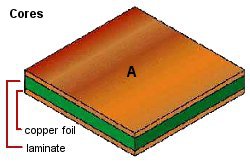
A) Cores
A laminate material is very thin, its thickness is normally under 0.025", it consists of glass epoxy substrate with copper on both sides.
Laminate is cut into the optimum panel size to accommodate the size of the particular PCB, and then its surface will be cleaned for the upcoming series of inner layer process.
Inner layer process: is to form inner layer circuitry of PCBs, which involves a series of process, like dry film resist coat, exposure, resist developing, etching, stripping resist, automatic optical inspection, oxide coating and lamination.
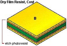
B) What is Dry Film Resist, Coat?
It is a UV light sensitive film, which is placed at the copper surfaces of the core, by heat and pressure.
Artwork(photo tools) will be placed on the dry film coated surfaces of the core. The artwork patterns are designed by customer that particular for each of their projects/ part number. Indeed, each surface has its own artwork pattern.
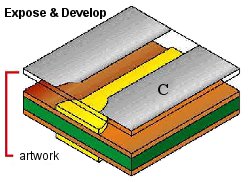
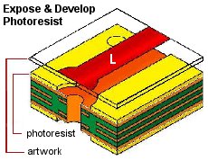
C) Expose & Develop
This process produces the image of the circuitry pattern onto the photo resist.
The exposed core is passed through a chemical solution removing the resist from areas not hardened.
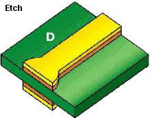
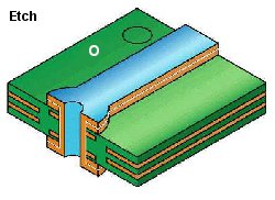
D) Etching
The unwanted copper to be chemically etched from the core in all areas not covered by film resist. Then, a discrete copper pattern will be occurred.
Core surface now shows through in area where copper was etched away.
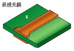
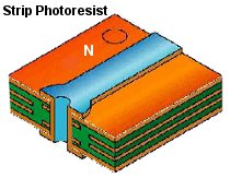
E) Finally, all the photo resist is stripped, to from the inner layer circuitry of PCBs.
To ensure the quality of the circuitry, the panels have to go through Automatic Optical Inspection(AOI).
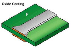
F) Oxide coating will be applied to enhance the bonding strength of the surface during the lamination cycle.
How? Copper is chemically treated to "rough-up" surface. Rough surface improves the bonding strength of the surface during the lamination cycle.
G) Lamination is a critical process in laminating inner layer(s) into multi layer PCBs. The inner lay up step can be found in this process.
Material needed for multi layer Lamination: Copper foils, Prepregs & Cores
H) Lay up step is to pile up the oxidized inner layer Cores according to the mentioned inner layer construction of PCB; prepreg material is required to insert in between any two layers, it acts as a multi-layer "glue". Copper foil is typically used for constructing the outer layers.
Inner layer cores, copper foil, prepreg are bonded together under high temperature and pressure, usually in a vacuum, during the pressing operation.
I) A laminated panel is formed after the lay up step.
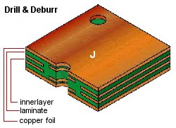 J) Drilling process takes place, holes are mode in the laminate panel so that electrical connection can be existed by the upcoming copper plating process among the specific layers of circuitry.
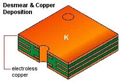
K) After drilling, desmear & deburr is another step to keep clean of the hole wall and the panel surface.
-- Desmear is a chemical process where the coating of resin, produced by the heat of drilling, is removed from the hole wall.
-- Deburr, a mechanical process where copper burrs are removed from the panel surface, & all debris are cleaned from drilled holes.
L) Copper deposition, it is also known as electroless copper. A thin coating of copper is chemically deposited on the surface of the panel and hole walls.
This creates a metallic bases for subsequent electroplating operations.
L) The image transfer process takes place, it is similar to that of the inner layer process in the following series of procedures, including dry film photo resist coat, photo resist exposure, resist developing,
M) electrolytic copper and tin N) stripping resist, O) etching unwanted copper and tin stripping, is involved.
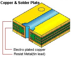
Additional copper is electrically plated onto the exposed copper surfaces. Tin is also plated onto all copper surfaces.
Unwanted copper is now removed any place not covered by tin.
Traces & pads, as defined by thy artwork, are now left on the surface of the panel.
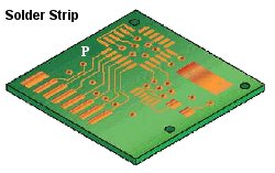
Tin, acting as resist, is chemically stripped from all surfaces producing a bare copper panel.
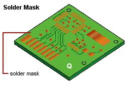
Q) The solder mask process, forms a protective coat of insulation over the PCB panel against contamination, handling damage and to facilitate subsequent assembly.
After the cleaning process, layer of solder mask is printed on the panel through curtain coating or silkscreen printing, and the same is subject to exposure for developing to create the image of the circuitry pattern.
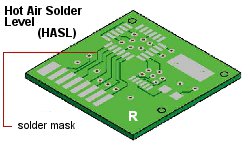
R) Selective surface finish, this process is to create a coating that is required for bonding the electrical components or parts onto the PCB, over certain parts of the circuitry depending on the design.
HASL(one of the typical surface finishes) PCBs are processed through a bath of molten solder, covering all exposed copper surfaces.
High pressure hot air, directed at both sides of the PCB simultaneously, clear up excess solder from the holes and surfaces.
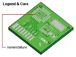
Then, S) ink is silkscreened onto each side of the PCB, as described by customer artwork.
The printing details component placement & other surfaces details requested by the customer.
PCB is baked to cure the ink. 
T) Profiling
The board is routed/punched to desired outline, this operation also known as profiling, it includes the following processes: punching with die, routing with machine, V-cutting for the later breakage, chamfering for better handing.
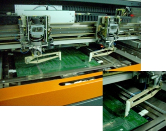
U) Electronic Test board is tested for electrical integrity, and if required, impedance. It is an open short testing. 
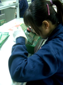
V) Final inspection is the last, but crucial process for Elec & Eltek to deliver out reliable completed PCBs. This process includes visual inspection, warpage test. Finally, the PCBs are packed and shipped according to customers' requirement.
 Please feel free to contact us for any further Questions...