|
FAQ
PCB Cost
|
1. Is it ok that I use another software beside Eagle to generate the Gerber files?
-- Yes, you can. Please make sure the gerber files include the following layers.
Top Layer: pcbname.GTL
Inner Layer: pcbname.GL2 (for 4-layer board)
Inner Layer: pcbname.GL3 (for 4-layer board)
Bottom Layer: pcbname.GBL
Solder Mask Top: pcbname.GTS
Solder Mask Bottom: pcbname.GBS
Silkscreen Top: pcbname.GTO
Silkscreen Bottom: pcbname.GBO
Drill Drawing: pcbname.TXT
Board Outline:pcbname.GML/GKO
2. How to export the drill files correctly?
Please select EXCELLON instead of Gerber_RS274X when choosing the Device for Drill Data, this will help you eliminate the size problem.
If you use Altium, .TXT & .DRL are both acceptable.
3. What is the minimum milling slot?
-- 1mm*2mm
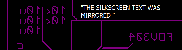
4. What is the correct way to draw the silkscreen on the bottom side?
Please make sure the silkscreen is reflected on the bottom side. Please refer to the picture below.
5. What are the PCB order status?
Confirmed: Your order is placed successfully.
PCB Processing: Your PCB order is under processing which include gerber verifying + production (normally this status will stay for 4-6 days).
In production: Your board has been finished and under quality check process. (normally this status will stay for 1 days).
Pending: Your PCB order is interrupted for reasons.
Shipped: Your order is collected for assignment by the forwarder.
Traceable: Tracking information for your order is available.
6.If my PCB do not require Solder Mask, what should I do?
Please add solder mask opening in Solder Mask Layer (GTS& GBS).Thanks!
7.If my PCB do not require Drilling Holes?
Please add an empty Drilling File in Gerber. Thanks!
8.Can I panelize thePCB?
Yes. But the sub-boards should only be separated by the silkscreen. Using any holes or slots to separate the sub-boards is not permitted. And the board outline needs to go all the way around the edge of the board (GKO or GML).
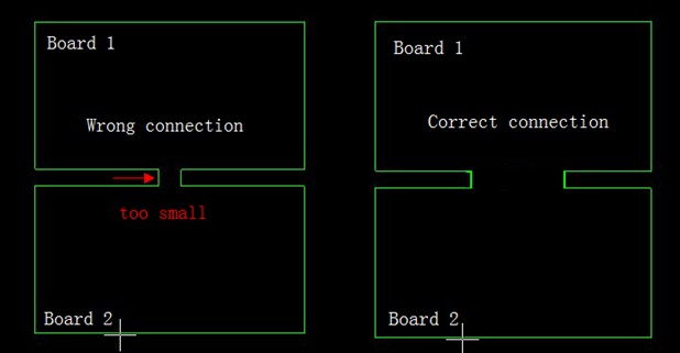
9.Can I use connection to panelize the board?
Yes. But the width of the connection should be 1/3 of the width of the board. For example:
10.Which layer I use in EAGLE for milling?
layer 46, but you need to add a note there
11.What is the minimum dimension of the boards/PCB for milling?
1*2mm
12.Is PCB panelization only for the same PCBs, or I can Panelize different PCBs?
Yes,you can panelize different boards together in one gerber. But should be less than 5 different boards within the size you choose.
13.For order over $50, is it free shipping?
Please note that we have changes on shipping service.
If you bought propagate service (fusion PCB, PCBA prototype, Laser cutting & Stencil), no free shipping on $50+.
Normal product (50+) + propagate service , free shipping on normal product.
normal product (50+) only, free shipping
Sorry for the inconvenience.
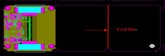
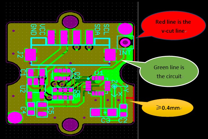
14.How should the V-cut line look like in Gerber?
In gerber, no space between boards. The board outline will be the v- cut line.
15.If Ihave the v-cut, what is the minimum length between circuit wire and the v-cut line?
More than 0.4mm.
16.What is the depth of the v- cut?
Normally, the depth of the v-cut this 1/3 thickness of the board. thetolanrence is+-0.5mm.
17.Canthe V-cut line be curve?
No, V-cut line can only be straight line.
18.What is the minimum dimension of the boards/PCB for panelization?
Only size over 8 cm * 8 cm can be applied V-cut / Panelization.
19.Which layer should I use in EAGLE for V-slot?
layer 50, but you need to add a note there.
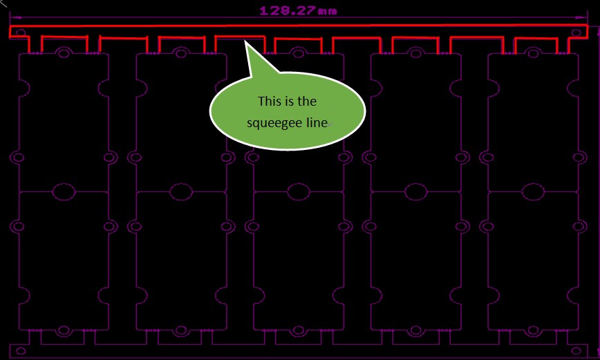
20.What is squeegee side / line ?
Standard PCB service
1-2 Layers
| 5 * 5 cm MAX |
0.6-1.6mm |
Green |
HASL |
100% E-test |
10 pcs |
$9.9 |
Discount |
| 5 * 10 cm MAX |
0.6-1.6mm |
Green |
HASL |
100% E-test |
10 pcs |
$12 |
Discount |
| 10 * 10 cm MAX |
0.6-1.6mm |
Green |
HASL |
100% E-test |
10 pcs |
$15 |
Discount |
Please note : Copper thickness 1 oz
4 Layers
| 5 * 5 cm MAX |
0.6-1.6mm |
Green |
HASL |
100% E-test |
10 pcs |
$55 |
Discount |
| 5 * 10 cm MAX |
0.6-1.6mm |
Green |
HASL |
100% E-test |
10 pcs |
$75 |
Discount |
| 10 * 10 cm MAX |
0.6-1.6mm |
Green |
HASL |
100% E-test |
10 pcs |
$85 |
Discount |
Please note : Outer Copper thickness 1 oz , inner copper thickness 0.5oz .
Standard PCB + additional specification service
This service allows you to design PCB considering 2oz copper thickness , ENIG surface treatment , impedance , color solder mask ( black ,white ,yellow ,red , blue , purple) , v-cut PCB , panelize PCB ,you can get this service with additional cost , which is various on your gerber design and quantity .
Custom PCB service
This service allows you to order PCB with 50 pcs >=quantity > =3 pcs , PCB size must >10 cm , any shape is availale .The price is based on the specification .
Small Batch PCB
When the purchased quantity is up to 50 pcs or more , that means the total area is a little big . So we calculate the PCB cost according to area . Ie ( PCB area x $70 / m2 + E-test fee ) x discount .
|