|
PCB Design
Parts Vs PCB
microelectronic
Altium
|
1. Reasonable layout power filtering / decoupling capacitors: General in the schematic drawing only some power filtering / decoupling capacitors, but pointed to where they should be connected to each. In fact, these capacitors are switching devices (gates) or other needs filtering / decoupling of components and settings, arranged these capacitors should be as close to these component parts, too far away, there is no a role. Interestingly, when reasonable power filtering / decoupling capacitor arrangement, the ground point of the question is not so obvious.
2. Line with stress: Conditional wide line never do meticulous; high voltage and high frequency lines should park slide, not a sharp chamfered corner nor right angle. Ground should be as wide as possible, it is best to use a large area of copper, which is the docking site issues improved considerably.
3. Have a reasonable trend: as input / output, AC / DC, strong / weak signal, high-frequency / low frequency, high-pressure / low pressure, etc ... They should be a linear trend (or separation), not each other blend. Its purpose is to prevent mutual interference. The best to be a straight line, but generally not easy to achieve, the most unfavorable trend is a ring, but fortunately you can set the isolation brought about improvements. For DC, small signal, low voltage PCB design requirements can be lower. Therefore, the "reasonable" is relative.
4. Choose a good grounding point: I do not know how many little ground engineering and technical personnel have done it much exposition, which shows its importance. Under normal circumstances require common point ground, such as: multiple forward amplifier ground wire should be connected to the mains and then converge and so on .... In reality, due to various constraints is difficult to completely done, but should try to follow. This problem is very flexible in practice. Everyone has their own set of solutions. As can be for a specific board to explain it is easy to understand.
5. Although some problems occurred in post-production, but it is caused by the PCB design, they are: too over the line hole, copper process slightest mistake will lay hidden. Therefore, the design should minimize the hole over the line. With the parallel lines of the density is too big, it is easy to weld together into one. Therefore, the linear density should be considered to determine the level of the welding process. Distance spot is too small, is not conducive to manual welding, can only be resolved in order to reduce the quality of welding efficiency. Otherwise it will stay hidden. Therefore, to determine the minimum distance of the solder joint quality and efficiency should be considered welding personnel.
6. Pad or over the line hole size is too small, or the pad size and drill size mismatch. The former artificial drilling unfavorable latter CNC drilling disadvantage. The pad is easy to drill into a "c" shape, while drilling off the pad. Wire too thin, and a large area of unrouted district has not set copper, likely to cause corrosion uneven. That is, when not finished wiring area of corrosion, thin wire corrosion is likely overdone, or similar non-broken off, or completely off. So, set just to increase the role of copper ground area and interference. The reliability of the above factors will be compromised on the quality of the board and future products.
How to choose packaging of components correctly when do layout
All the examples in this article were developed using multisim design environment, but even using different eda tools, the same concept still applies.
1. Use a good grounding method
Ensure that the design has sufficient bypass capacitor and the ground plane. When using the integrated circuit, ensure that the location close to the supply terminal to ground (preferably ground plane) using the appropriate decoupling capacitors. Suitable capacitance depends on the particular application and operating frequency capacitive technology. When the bypass capacitors placed between the power and ground pins and pins placed near the right IC can optimize electromagnetic compatibility and susceptibility of the circuit.
2, assign a virtual component packaging
Print a copy of the bill of materials (bom) is used to check the virtual components. Virtual elements are not related to the package, not transferred to the layout stage. Create a bill of materials, and then view the design of all the virtual components. The only entry should be power and ground signals, because they are considered a virtual device, only specific treatment in the schematic environment, not transferred to the layout design. Unless used for simulation purposes, part of the display elements in the virtual element should be used to replace with a package.
3. Make sure you have a complete bill of materials data
Check the material if there is a complete inventory report enough data. After you create a bill of materials report, should be carefully examined for all components of the device is incomplete entries, supplier or manufacturer information to complete it.
4, reference numeral sorted according element
To help sort and view a list of materials to ensure the element labels are consecutively numbered.
5, check the extra gates
In general, all the extra doors should have a signal input connection, to avoid floating inputs. Make sure that you check out all the redundant or missing gates, and all inputs are absolutely no connection even on. In some cases, if the inputs are in a suspended state, the entire system can not work properly. Take the design often use dual op amps. If dual op amp IC elements used only one operational amplifier, suggested either to another op amp also use them, or will not have the op amp's input is grounded, and laying a proper unity gain (or other gain ) feedback network to ensure that the entire device to work properly.
In some cases, there is a suspension pin IC may not work properly in the target range. Usually only when the IC device or the same device in the other doors are not working in saturation - the input or output power rails near or in components, in order to meet the requirements of this IC indicators work. Simulation generally can not capture this case, since the simulation model is generally not a plurality of portions of the IC are connected together for connection modeling suspension effect.
6, consider the component package choice
Throughout the schematic drawing phase, you should consider component packaging and landpattern need in the layout stage decision. Here are some recommendations when selecting components based on component packages need to be considered.
● Keep in mind, the package includes an electrical and mechanical connection pad dimensions (x, y, and z) elements, i.e., the shape of the element body and the pin connections of the PCB. When selecting components, you need to consider any installation or packaging constraints final PCB top and bottom may exist. Some components (if any polar capacitor) may have a high degree of headroom limitations need to be considered in the component selection process. In the initial start of the design, you can draw a basic circuit board frame shape, and then placed on a large or location you plan to use some of the key elements (such as the connector). Thus, you can quickly and intuitively see (no wiring) boards a virtual perspective, and gives the relative positioning and component height relatively accurate circuit boards and components. This will help to ensure that after PCB assembly components can be placed in the appropriate packaging (plastic products, chassis, chassis, etc.) inside. Three calls from the Tools menu in preview mode you can browse the entire board.
● land pattern shows the actual PCB solder pads on the device or via shape. These copper pattern on the PCB also contains some basic shape information. The need for proper land pattern dimensions to ensure proper welding, and to ensure that the connected components correct mechanical and thermal integrity. PCB layout design, you need to consider how the board will be manufactured or hand soldering, then how will the welding pad. Reflow (solder melts at a controlled temperature furnace) can handle a wide variety of surface-mount devices (smd). Wave soldering is generally used to the opposite side of the board to fix the through-hole devices, but can also handle some of the tables placed in the back of the PCB-mount components. Typically when using this technique, the underlying surface mount device must be arranged in a particular direction, and in order to adapt to this welding method, you may need to modify the pad.
● Throughout the design process can change the selected element. Early in the design process is to determine which components should be plated through holes (pth), which should be used surface mount technology (smt) will contribute to the overall planning of the PCB. Factors to consider are the device cost, availability, and so the device area and power density. From a manufacturing perspective, surface-mount devices are typically cheaper than through-hole devices, and higher general availability. For small-scale prototype of the project, the best selection of larger surface-mount or through-hole devices devices, hand soldering is not only convenient, but also to facilitate troubleshooting and debugging process better connection pads and signals.
● If the database does not have ready-made package, usually create a custom package in the tool.
Introduction and analysis of new microelectronic packaging technology
1 Introduction
Circuit industry has become the key to national economic development, and integrated circuit design, manufacture and IC packaging and testing industry is the pillar industry of the three. It is the consensus of all levels of leadership and industry. Microelectronics Packaging not only directly affect the IC itself, electrical, mechanical, optical and thermal performance, affecting its reliability and cost, is still largely determines the electronic machine system miniaturization, multi-functional, reliability and cost, microelectronic packaging more and more widespread attention in the international and domestic is in a boom phase. This paper attempts to overview the rapid development of new microelectronic packaging technology since the 1990s, including ball grid array package (BGA), chip scale package (CSP), wafer-level packaging (WLP), three-dimensional packaging (3D) and system in Package (SIP) items of technology. Introduce their development status and technical characteristics. At the same time, describes the concept of the three microelectronic package. And made a number of proposals to develop our thinking and new microelectronic packaging technology. This paper attempts to overview the rapid development of new microelectronic packaging technology since the 1990s, including ball grid array package (BGA), chip scale package (CSP), wafer-level packaging (WLP), three-dimensional packaging (3D) and system in Package (SIP) items of technology. Introduce their development status and technical characteristics. At the same time, describes the concept of the three microelectronic package. And made a number of proposals to develop our thinking and new microelectronic packaging technology.
2 Microelectronics three packages
Microelectronic packaging, we need to describe what the concept of the three packages. In general, divided into three microelectronic packaging. The so-called primary package is a semiconductor wafer after the lobes, one or more integrated circuit chips with a suitable package encapsulated, and the chip pad and package pin-out by wire bonding (WB), the carrier tape automated bonding (TAB) and flip chip bonding (FCB) to link up to become practical function of electronic components or assemblies. Package includes a single-chip module (SCM) and multi-chip module (MCM) into two categories. Three packages that will be two packages of products through selected layer interconnection socket or flexible circuit board and the motherboard linked together to form a three-dimensional packaging, a complete machine system, which should include a package connectors, laminated flexible circuit board assembly and other related materials, design and assembly technology. This is also known as a system-in-package. The so-called microelectronic package is full of concepts, including a package from one pole to pole all the technical content of the three packages. We should recognize the existing track into international microelectronic packages, both for China's microelectronics packaging industry and technological exchanges with foreign countries, but also conducive to the development of microelectronic packaging itself.
3 new microelectronic packaging technology
History IC packaging, and its development is mainly divided into three stages. The first phase, before the 1970s, mainly to plug type package. Including the original metal circular (TO type) package, and later ceramic dual in-line package (CDIP), Ceramics - Glass dual inline package (CerDIP) and plastic dual in-line package (PDIP). Especially PDIP, due to excellent performance, low-cost mass production can become a mainstream product. The second phase, after the 1980s, with the four sides of the surface mount type lead-based packages. At that time, the surface mount technology is called a revolution in the field of electronic packaging, has been developing rapidly. With suitable, a number of surface-mount packages to adapt to technology, such as plastic leaded chip cut body (PLCC), plastic sides lead flat pack (PQFP), plastic small outline package (PSOP), and quad flat no-lead package, etc. package emerged rapidly. Due to the high density, lead pitch, low cost and suitable for surface mounting, make PQFP become the dominant product in this period. The third phase, after the 1990s, mainly in the form of area array packages. Thin-film multilayer substrate MCM (MCM-D), plastic multilayer printed MCM (MCM-L) and thick film substrate MCM (MCM-C / D).
3.13D package
There are three main types of 3D packaging, namely embedded type 3D package, currently there are three main ways: one is in the various types of substrate dielectric layer or multi-layer wiring "buried" R, C or IC and other components, the top again SMC and SMD placement to achieve three-dimensional packaging, this structure is called a buried-type 3D package; the second is on the active substrate such as silicon wafer-scale integration (WSl) again after the implementation of a multi-layer wiring, the top and then mount SMC and SMD, which constitutes three-dimensional packaging, this structure is called the active substrate type 3D packaging; the third is based on 2D package, the plurality of bare chips, packaged chip, multi-chip module or laminated wafer interconnected to form three-dimensional package, such a structure is called stacked 3D packaging. In these types of 3D packaging, is the fastest growing stacked die package. There are two reasons. First, the huge mobile phones and other consumer-driven market, requiring increasing functionality while thinning package thickness. Second, it uses basically compatible with the traditional craft techniques, improved production and into the market very soon. It Prismarks predict mobile phone sales in the world from 2001 to 2006, 393M 785M ~ 1140M. Annual growth rate of 15 to 24 percent. So on this basis is estimated stacked die package from now until 2006 will be increased by 50 to 60% faster. Figure 6 shows a stacked die package outline. Its current level and trends are shown in Table 3.
There are two stacked stacked die package, one is the pyramid, from the ground up smaller die size; the other is the cantilever type, as big chip stack size. Early used in mobile phones, and stacked die packages mainly to FlashMemory and SRAM stacked together, has been able to FlashMemory, DRAM, logic IC and analog IC and other stacked together. Key Technology stacked die package has the following involved. ① wafer thinning technology, mobile phones and other products require increasingly thin package thickness, currently packaged in a 1.2mm thickness requirements even below 1.0mm. While also increasing the number of stacked chips, thus requiring the chip must be thinned. Wafer thinning methods include mechanical polishing, chemical etching or ADP (Atmosphere DownstreamPlasma). Mechanical polishing thinning generally about 150μm. The ion etching method, etc. can be reached 100μm, for 75-50μm thinning under development; ② low arc bond, because the chip thickness is less than 150μm, so the bond must be smaller than the curvature of high 150μm. Currently using 25μm gold wire bonding normal arc height 125μm, and after using the reverse wire bonding process can be optimized to achieve high arc 75μm or less. At the same time, the reverse wire bonding technology to add a process to ensure that the gap clinchers different bonding layer; ③ cantilever wire bonding on the cantilever longer, the greater the deformation of bonding the chip, the design must be optimized and technology; ④ wafer bumping technology; ⑤ bonding wires no swing (NOSWEEP) molding technology. Since the wire bonding higher density, the length of the longer, more complicated shape, increasing the likelihood of a short circuit. Using a low viscosity molding compound and reducing the transfer speed of the molding compound helps to reduce the bonding wire wobble. Present invention, the bonding wire has non-wobbled (NOSWEEP) molding techniques.
3.2 ball grid array package (BGA)
Array package (BGA) is the world's developed in the early nineties a new package.
Advantages BGA package I / O terminals with round or columnar joints distributed in a matrix form below package, BGA technology is the I / O pin count, although increased, but the pitch is not reduced but increased, thus improving the assembly yield; although its power consumption increases, but can be controlled collapse chip BGA soldering method, which can improve its electric performance; the thickness and weight of packaging technology than the previous decline; reduce parasitics, signal transmission delay is small, the frequency of use is greatly improved; available coplanar welding assembly, and high reliability.
The outstanding advantage of this BGA: ① electrical properties better: BGA solder balls instead of lead, a short path leads to reduced pin delays, resistors, capacitors and inductors; ② higher packaging density; the balls are arranged throughout the plane , so for the same area, a higher pin count. For example, the side length of 31mm BGA, have 900 pins when ball pitch of 1mm, by contrast, the side length of 32mm, 0.5mm pin pitch of only 208-pin QFP; ③BGA's Day distance of 1.5mm, 1.27mm, 1.0mm, 0.8mm, 0.65mm and 0.5mm, is fully compatible with existing surface mount technology and equipment, the installation is more reliable; ④ due to the surface tension when the solder melts "self-alignment "effect, to avoid the traditional package leads deformation losses, greatly improving the assembly yield; ⑤BGA pin solid, easy transport; ⑥ balls drawn form is equally applicable to multi-chip packaging components and systems. Therefore, BGA been explosive growth. BGA substrate material varies with plastic ball grid array packages (PBGA), ceramic ball grid array package (CBGA), a metal ball grid array carrier tape ball grid array package (TBGA), ball grid array package with a heat sink (EBGA), package (MBGA), as well as flip-chip ball grid array package (FCBGA.PQFP may be applied to surface mounting, which is its main advantage, however, when the lead pitch PQFP reaches 0.5mm, its technical complexity of the assembly will increase in the lead more than 200 and the number is greater than the size of more than 28mm square package applications, BGA replace PQFP package is inevitable. in the above categories BGA package, FCBGA most want to be the fastest growing · BGA package we wish to it, for example, describes the BGA technology and materials in addition to all the advantages of .FCBGA BGA also has: ① excellent thermal performance, the chip can be mounted on the back of the radiator; ② high reliability, due to lower chip packing the role of the fatigue life is greatly enhanced FCBGA; ③ can rework strong.
Because the board is already equipped with other surface mount components, it is necessary to adopt special small BGA template, thickness and size of the opening to be determined by the diameter of the ball and the ball away, you must check the print quality after printing is completed, such as failure, must be cleaned PCB clean and dry again after printing. For ball pitch of CSP 0.4mm or less, the solder paste may not be printed, it is not necessary to use rework processing templates, brushing directly paste flux on the PCB pads. PCB components need to split into the oven, the press reflow bond, and other machines by setting the program to finish at the highest temperature in and out when you press the key, remove the element to be removed with a vacuum suction pen, PCB board cooling can be.
Key Technology FCBGA involved include chip bumping technology, flip-chip bonding technique, a multilayer printed circuit board fabrication techniques (including the multilayer ceramic substrate and a BT resin substrate), the bottom of the chip padding technique, a solder ball attachment technique, heat plate attachment technology. It involves encapsulating materials include the following categories. Bump material: Au, PbSn and AuSn and the like; metal material under bump: Al / Niv / Cu, Ti / Ni / Cu or Ti / W / Au; Welding Materials: PbSn solder, lead-free solder; multilayer substrate material : High-temperature co-fired ceramic substrate (HTCC), low temperature co-fired ceramic substrate (LTCC), BT resin substrate; underfill material: liquid resin; thermal plastic: Silicone; radiating plate: copper.
3.3 chip scale package (CSP)
CSP (Chip Scale Package) package, chip scale package meant. The latest generation of memory CSP package chip packaging technology, its technical performance has a new promotion. CSP CSP package installed seal that allows the chip area and packaging area ratio of more than 1: 1.14, is already quite close to 1: 1 in the ideal case, the absolute size is only 32 mm2, which is about 1/3 of an ordinary BGA, quite simply TSOP memory chip area to 1/6. Compared with the BGA package, the same space CSP package can be up to three times the storage capacity.
Chip Scale Package (CSP) and BGA is a product of the same age, is the whole compact, portable results. JEDEC to define American CSP is: LSI chip package size is less than or equal to 120% of the area of the LSI chip package called CSP. Because many in the form of CSP BGA, so packaging industry pundits believe the last two years, greater than or equal lmm ball pitch for BGA, less than lmm for CSP. Because CSP has a more prominent advantages: ① approximate chip ultra-small package size; ② protect the bare chip; ③ electrical, thermal excellent; ④ high packing density; ⑤ facilitate testing and aging; ⑥ easy welding, installation and repair replacement. Thus, the mid-nineties to get large-span development, growth about twice a year. Because CSP is in a boom phase, so it's kind of more limited. Rigid substrates such as CSP, flexible substrate CSP, lead frame type CSP, micro molding type CSP, pad array CSP, micro BGA, bump chip carrier (BCC), QFN type CSP, chip lamination wafer level CSP and CSP (WLCSP) and the like. CSP pin pitch of 1.0mm or less in general, there are 1.0mm, 0.8mm, 0.65mm, 0.5mm, 0.4mm, 0.3mm and 0.25mm and the like. Table 2 shows the CSP series.
Generally, CSP, is the wafer into individual IC chips and then, after the implementation of the package, and WLCSP is different, it's all or most of the process steps in the process have been completed before the completion of a silicon wafer, and finally direct wafer is cut into separate stand-alone devices. So this package is also known as wafer level packaging (WLP). Therefore, in addition to the common advantage of CSP, it also has unique advantages: ① high encapsulation processing efficiency can simultaneously process multiple wafer; ② with flip-chip packaging advantages, namely light, thin, short, small; ③ and compared to the former process, only increased the lead to re-routing (RDL) and bumping two processes, all the rest is the traditional process; ④ reduce the traditional packaging of several tests. Therefore, the large IC packaging companies in the world have invested in this type of WLCSP research, development and production. WLCSP deficiency is low pin count, there is no standardization and higher costs.
Center pin in the form of memory chip CSP package effectively shortening the distance the signal transduction, the attenuation reduced, chip jamming, anti-noise performance can be significantly improved, which also makes CSP BGA improve access time than 15 % -20%. In CSP encapsulation mode, the memory chips are soldered by solder balls one by one on the PCB board, due to the larger contact area and the PCB pads, memory chips so the heat generated in the operation can be easily conducted to the PCB board and dissipated. CSP package from the back of the radiator, and a good thermal efficiency, CSP thermal resistance of 35 ℃ / W, while the thermal resistance TSOP 40 ℃ / W.
CSP technology is presented at the time of replacement of electronic products to come, it is aimed at the use of large chips (chips more features, better performance, more complex chips) instead of the previous small chip, its occupancy package printing plates area remains unchanged or less. It is because the package CSP product is small, thin, and therefore it is a handheld mobile electronic device to obtain the application rapidly. In August 1996, the Japanese company Sharp began mass production of CSP products; CSP product assembly cameras in September 1996, Sony Corporation of Japan began TI and NEC Corporation of Japan provided; in 1997, the United States also began production of CSP products . There are dozens of companies in the world can offer CSP products, all kinds of product variety CSP many as 100 or more. [
The key technologies involved WLCSP besides the first step necessary for the metal deposition technique, a photolithography technique, an etching technique, etc., further comprising re-wiring technology (RDL) and bumping technology. Typically terminals pads on the chip are discharged at the die around the square aluminum layer, in order to adapt to the SMT secondary WLP package wider pad pitch, the need to re-distribution of these pads, these pads by chip to chip around the arrangement of the active surface of the array arrangement, which requires re-wiring (RDL) technology. Solder bumping technology can be electroplating, electroless plating, evaporation, set the ball and solder paste printing method. Plating method is currently still the most widely used, followed by solder paste printing method. Rewiring the UBM material Al / Niv / Cu, T1 / Cu / Ni or Ti / W / Au. Dielectric material used is a photosensitive BCB (benzocyclobutene) or PI (polyimide) bump materials are Au, PbSn, AuSn, In and the like.
3.4 System in Package (SIP)
Achieve functional electronic machine system, there are usually two ways. One is the system-on-chip (Systemon Chip), referred to as the SOC. That is implemented on a single chip functions electronic machine system; the other is a system-in-package (SysteminPackage), referred to as SIP. That is achieved by encapsulating the function of the whole system. From an academic perspective, this is the two technical routes, as monolithic and hybrid integrated circuits, as each have their own advantages, each have their own applications. Technically and applications are mutually complementary relationship, the authors believe, SOC should be mainly used for a longer period of application of high-performance products, and SIP applications mainly for short-cycle consumer products.
An important feature of SIP is that it does not define the type of session to be established, but only defines how to manage the session. This flexibility means that SIP can be used in many applications and services, including interactive games, music and video on demand as well as voice, video, and Web conferencing. SIP messages are text-based, and thus easier to read and debug. Programming of new services easier and more intuitive for designers in terms. SIP as e-mail client, like reusing MIME type description, and therefore associated with the application can automatically start the session. SIP reuse some existing mature Internet services and protocols such as DNS, RTP, RSVP, etc.
SIP is more flexible, scalable, and open. It inspired the Internet as well as fixed and mobile IP network to launch next-generation services in power. SIP messages on the network can be completed more than one PC and phone, simulating the Internet to establish a session.
SIP is the use of sophisticated assembly and interconnection technology to a variety of integrated circuits, such as CMOS, GaAs circuits, SiGe circuits or optoelectronic devices, MEMS devices and a variety of passive components such as capacitors, inductors integrated into one package, bring the whole functional machine systems. The main advantages include: ① the use of existing commercial components, lower manufacturing costs; ② products into the market cycle is short; ③ regardless of design and technology, there is greater flexibility; ④ the different types of integrated circuits and components , relatively easy to implement. Georgia Institute of Technology Research and Development PRC single-level integration module (SingleIntegrated Module) called SLIM, SIP is a typical representative of the project is completed, 10-fold increase in packaging efficiency, performance and reliability, the larger the size and cost reduction. 2010 is expected to reach the goal, including wiring density of 6000cm / cm2; heat density of 100W / cm2; component density 5000 / cm2; I / O density of 3000 / cm2.
Although SIP is a new technology is not yet mature, but still is a promising technology, especially in China, could be a shortcut to the development of the whole system.
4 Thoughts and Suggestions
Faced with microelectronic packaging booming world situation, analyze the current status quo, we must ponder some problems.
A high degree of importance to the vertical integration of microelectronics three packages. We should as a leader in electronic systems, affecting one, two and three packages can only dominate the market, improve economic efficiency and development. We have encouraged the phones and radar as a technology platform for the development of the microelectronics packaging, is out of this consideration.
Second, attaches great importance to the cross and the integration of different areas and technologies. Cross and integration of different materials to produce new material; crossover and convergence of different technologies to produce new technologies; crossover and integration of different areas to generate new fields. In the past, the industry communicate a lot, but not enough to communicate in different industries. We should give full play to the role of each branch of the Institute of Electronics, actively organize this technology exchanges.
Third, microelectronic packaging and electronic products are inseparable, has become a constraining the development of electronic products as well as the system's core technology, advanced manufacturing technology is one of the electronics industry, who gets it, who will master the future of electronic products and systems.
Fourth, microelectronic packaging must keep pace in order to develop. International Microelectronics Packaging history proves this point. How the times of microelectronic packaging? Our priority is to study the development of microelectronic packaging strategy, development planning. The second is to optimize the research and production of microelectronic packaging system. The third is to actively promote and develop our own intellectual property belonging to the original technology. Otherwise, we will track the more backward. At this point, we can well learn from the experience of South Korea and Taiwan.
Fifth, our ideas, technology and management must with international standards, and take the road of international cooperation, the essence of our nation and the wonderful world of one solution, and common development.
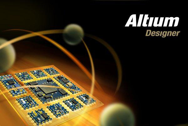
Analysis of Altium Designer, Fill, Polygon Pour, Plane and use different methods
Fill representation drawing a solid copper, the area connecting all wires and vias in one, regardless of whether it belongs to the same network. If the region has drawn both VCC and GND network connection Fill command to put this together, the two elements of the network, so it may cause a short circuit.
Polygon Pour: cutting copper pour area. Such as the need for irrigation to optimize or reduce copper, can be used to reduce the area is divided into two irrigation Line copper, copper pour area will not be deleted directly.
Polygon Pour Cutout: establish dig copper in copper pour area. For example, some important elements of the network or at the bottom of the processing needs to be hollowed out like a common RF signal, often requires hollowed handle. There transformers below, RJ45 area.
Polygon Pour: copper pour. Fill it with a similar role, but also draw a large area of copper; but the difference is that the "filling" word, copper pour a unique intelligence, will take the initiative to distinguish between copper pour the vias and solder networks. If vias with solder belong to a network that will be filling the copper vias, solder and copper together according to predetermined rules. On the contrary, it will keep a safe distance between the copper and vias and pads. Copper pour intelligence is also reflected in the dead of copper it is automatically deleted.
In summary, Fill will cause a short circuit, then why use it?
Fill even has its shortcomings, but it also has its environment. For example, LM7805, when AMC2576 chips and other high-current power supply, a large area of copper for chip cooling, you can only have one piece of copper on the network, using the Fill command will be just right.
So Fill command is often used in the early board design. After the layout is complete, use the Fill the special areas are drawn well, you can avoid mistakes in the design of subsequent species too.
In short, in the circuit board design process, the two tools are used in conjunction with each other.
Plane: plane layer (negative), applicable to the entire board is only one power or ground networks. If there are multiple power or ground network, you can draw a closed box with a line at a power or ground area, and then double-click the closed box corresponding to the regional distribution of power or ground networks, than add layer (positive layer ) can reduce the amount of data a lot of projects, in dealing with high-speed PCB faster reaction speed of the computer. in the process of revision or modification can be a profound experience of the benefits of plane.
Option 1: Select the desired copper trim, M + G shortcut keys can be adjusted copper shapes.
Option 2: When the repair copper can use PLANE [shortcut P + Y] to repair an obtuse angle.
|