There are two pieces of PCB fabricated from the factory , one is bad , the other one is good .How is the issue come to happen ? let's see below :
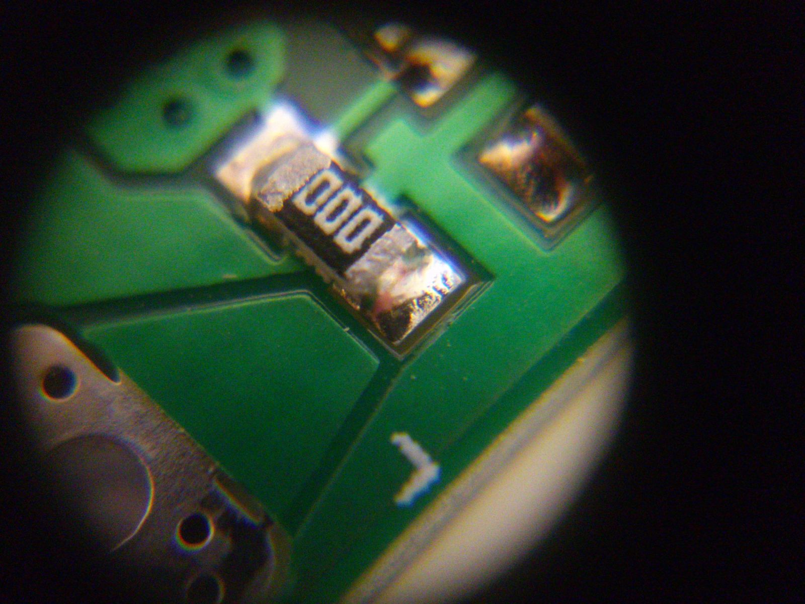
Good PCB
Defected PCB
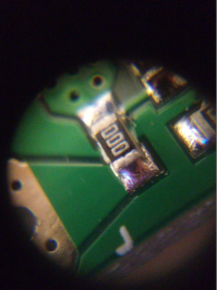
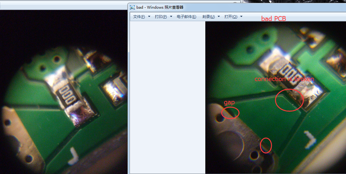
After companring them , do you notice any difference ? Yes , in the first picture , the connection is broken ,
How is that happen ?
Let's have a view on the original gerber file ,
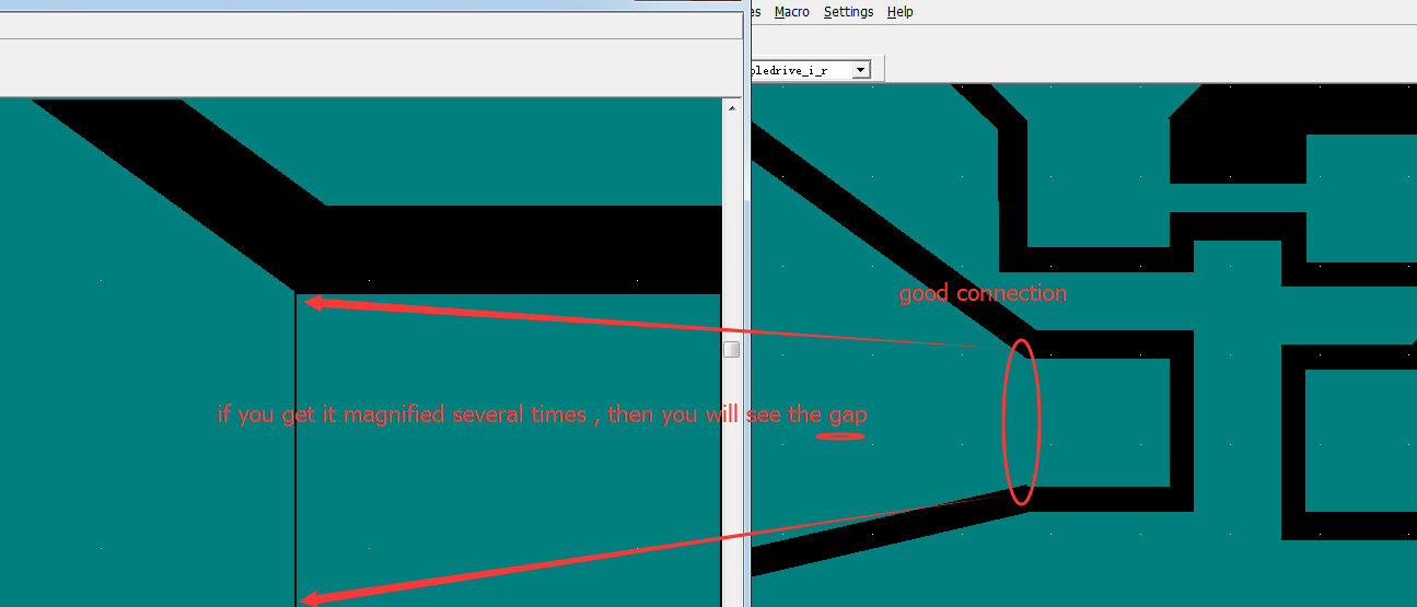
In the PCB factory , the enginners use Genesis 2000 to modify your gerber file . The engineer runs Genesis with function edited in C++ language . Some of them don't check the gerber file after modified by Genesis by accident .At this time , Genesis may possible to cut some connection because of the default action ( gap <2mil will be filled with copper or be broken ), then the bad production gerber file will be deliveried to production ,
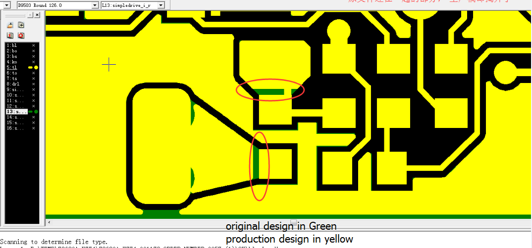
The engineer from the factory tell us , they pay more attention to the gap , some gap has to be filled , some gap has to be broken .How do they judge " filling " or " broken " ?
Sometimes , they analasis the circuit net by their experience , if the gap don't have any fuction , they will fill with copper or broken ; sometimes they rely on Genesis to fill copper or broke them .Mostly , they will compare the production file with original file in case too much difference on the production file . Unfortunately , there are 1-2% possibility that some production files are failed to be compared , and resultant with bad PCB .
I kindly suggest the one who do PCB layout , better have a strengthen view on your circuit gap . We also will ask our engineer to be more careful with it .
|