|
Common PCB Layer Types
Printed circuit boards have many different types of layers. To the uninitiated these layer types can be quite confusing, but once you have a basic understanding, you’ll see that it is all quite simple.
The figure below depicts a three dimensional view of a 4-layer PCB that has two routing layers (top and bottom) and two internal planes (GND and PWR). Don’t worry if that sentence doesn’t make sense to you right now, we’ll step through each of the common layer types in this article.

4-Layer PCB with 2 Routing Layers, a Ground Plane and a Power Plane
Below is a two-dimensional image of the same board with all layers shown on top of one another. Using this board as a reference, we’ll now dive into each of the common PCB layer types.
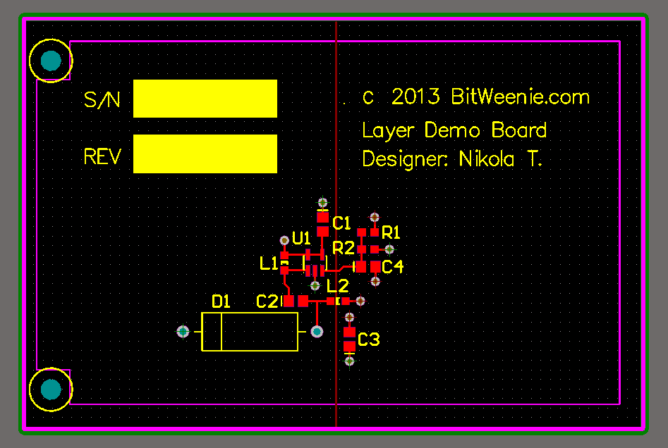
4-Layer PCB with all Layers Shown
Keep in mind that not every PCB contains all the layers listed – the need for different layer types depends on the specifics of your design. Single layer boards typically include: a mechanical layer, a keep out layer, a routing layer, an overlay layer, a solder mask layer and a solder paste layer. Multilayer PCBs contain those same layers as well as a mix of additional power planes, ground planes and more routing layers. The most common boards are 2-, 4- and 6-layer PCBs though it is not uncommon to have PCBs with over 12 layers.
Mechanical Layer

Mechanical Layer Shown in Pink
You may have multiple mechanical layers, but you will need at least one to fabricate your board. The most basic mechanical layer (sometimes referred to as Mechanical 1) outlines the physical dimensions of your board. This is depicted by the pink outline in the image above. The fabricator will use this layer to cut out your circuit board from their stock material.
This outline can be a simple rectangle or a more complicated shape with rounded corners and / or cut outs. While less common, additional mechanical layers are sometimes included detailing tooling specifications and other miscellaneous mechanical information. For most PCBs these additional mechanical layers are not needed though, so we won’t dive deeper into this topic.
Keep Out Layer

Keep Out Layer Shown in Pink
Where the mechanical layer defines the physical boundaries of your board, the keep out layer specifies constraints on the working area of your design. For example, you may want all components drawn back 1/2 inch from the perimeter of your board, the keep out layer will constrain your design in this manner. This is not a layer that is provided to the fabricator, but rather works with your design software to provide feedback to the designer as they develop their design to indicate whether or not they are in violation of the predetermined boundaries.
Keep outs aren’t restricted to the permitter of your board either, they can be used to identify segments on the interior that need to stay clear for mechanical or other reasons. In the image above the keep out restricts our working area from the outer edges of the PCB and near the two mounting holes on the left side of the board.
Routing Layers

Top Routing Layer Shown in Red
Routing layers are used for component interconnects. These are the layers that designers spend the majority of their time perfecting. Routing layers can be located on both outer (referred to as top and bottom layers) and internal layers on your PCB. These layers must be provided to your fabricator to create your board. The image shown above is the top PCB layer so in addition to the component interconnect routing, you also see the pads for the actual components.
Ground Planes & Power Planes

Ground Plane Shown in Green
Ground planes and power planes are solid copper layers shorted to a fixed potential. Very simply, ground planes are connected to GND and power planes are connected to one of your onboard voltages. Similar to routing layers, these can be located on the top, bottom or within the internals of your board.
These planes may seem boring, but they are both highly convenient for distributing power and ground across all of your components and may greatly benefit performance under certain conditions. Fabrication files describing all planes within your design must be provided when creating your custom PCB. In the above image the green outline depicts the ground plane – which is to say that it is a solid copper pour over the whole layer.
Split Planes

Split Power Plane Layer Shown in Maroon
Power and ground planes can be modified such that they contain multiple copper sections connected to different potentials. These further enhance the convenience of planes – consider a plane that has multiple voltages on it distributing +5V to one section of your board and -5V to another section. That is exactly the division in the image of the split power plane above.
The section on the left side of the line down the center of the board is connected to +5V while the section to the right is at -5V. There are a few performance issues to consider when splitting planes up, especially if it’s a ground plane. However, this topic is beyond the scope of this article, stay tuned for a future post on this subject.
Overlay (Silkscreen) Layers

Top Overlay Layer Shown in Yellow
Overlay or silkscreen layers provide, among other things, the text designators for your components on the top and bottom layers. If utilizing these layers, separate files should be provided to the fabricator for the top and bottom overlays. There is no need for overlays on internal layers (you’d never be able to see them!). If you don’t care to have text on your board, these files are not necessary. However, text is immensely helpful, especially when debugging boards in the lab.
For example, if you want to know the potential at one terminal of resistor R2, you simply find the text “R2″ printed on your board and probe. This is much easier than the more tedious option of referring back to your design on the computer or paper printouts. Overlay layers are also great for including your company name, design name, revision number and serial number of the board. Typically, blank boxes are printed for the revision and serial number so that they can be written in later with a sharpie or stamped onto the board.
Solder Mask Layers

Top Solder Mask Layer Shown in Purple
If you’ve ever seen a PCB you are no doubt familiar with their oddly green coloring. This thin green protective covering on the top and bottom of a PCB is called the solder mask and it helps protect traces from shorting when debris is present on your PCB. Not every board includes a a solder mask and there may be circumstances where you want a solder mask on the top layer, but not the bottom or vice versa (at high speeds there are some performance issues to consider with solder mask).
If you do go with a solder mask, you must provide files for all layers where this covering is desired (top and bottom are the only options). One final detail, solder masks are specified as negatives. In other words, areas that aren’t to be covered, will be filled in on your solder mask layer. This is apparent when examining the example solder mask image above. The only purple spots on the top layer are for component pads. Of course, we can’t have solder mask covering where our components need to make electrical contact with the board!
Solder Paste Layers

Top Solder Paste Layer Shown in Gray
Solder paste is a material used to assist in the soldering of surface mount components on a PCB. The pads on the surface mount components you use in your design will specify solder paste within the exposed copper region (not covered by solder mask). When the board is populated with surface mount components, solder paste helps the solder flow better as it bonds the component pin to the copper on your PCB.
Solder paste files are necessary for the top and bottom side of your design when using surface mount components on those layers. There are a handful of surface mount components on the top side of our example board so in the image above you’ll notice the gray coloring for solder paste on the pads for those components.
Conclusion
Printed circuit boards can be as simple as a single routing layer with a mechanical layer defining the physical dimensions of your board or as complicated as a multilayer board with all the layers outlined in this article. However, when considered individually, each layer has a very specific and simple purpose. Once you understand the purpose of each layer, understanding PCB construction becomes very simple no matter how complicated the board.
|